RESEARCH
December 2019
Takashi Tokuda1, Makito Haruta2, Kiyotaka Sasagawa2, and Jun Ohta2
1: Institute of Innovative Research, Tokyo Institute of Technology, Japan
2: Graduate School of Science and Technology, Nara Institute of Science and Technology, Japan
Corresponding author: Takashi Tokuda
E-mail: tokuda@ee.e.titecha.ac.jp
Since the rise of optogenetics, various types of optical stimulators have been proposed and realized. These include wired and wireless, single-site and multi-site, and with and without integration of other measurement / stimulation modalities. Naturally there is a trend to pursue very-small, light-weight devices that can be implanted or directly attached to animals. Such devices enable freely moving optogenetic experiments. Freely moving situations are preferred especially in behavioral experiments. Some research groups have been actively developing small, wireless, optogenetic stimulators [1-4]. Considering the importance of small size and lightness, most of the devices are developed with battery-less designs, meaning that power is wirelessly transferred during the operation. Realistic power transfer schemes for such devices are limited to either electromagnetic (RF-) or photovoltaic (PV-) powering.
Surveying preceding works, we observe that RF-powering is more actively employed than PV-powering. If we allow the size of devices to be larger than a couple of millimeters, it is reasonable to take the RF-powering approach as it has various advantages over PV-powering, and sufficient power transfer capabilities have been demonstrated. An ultra-small optogenetic stimulator equipped with a secondary (power-receiving) coil of approximately 2×2×2 mm3 was successfully demonstrated [3].
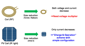
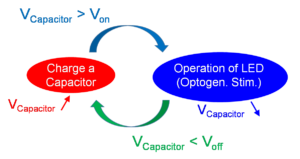
However, with a device of size 1 mm3 or smaller, we believe that PV-powering can be comparable, or even an advantageous alternative to RF-powering. Fig. 1 schematically compares RF-powering and PV-powering from the viewpoint of ultra-small implant technology. Generally, when we reduce the sizes of secondary power-receiving devices (antennae for RF, and PV cells for PV), the available electric power decreases. In RF-powering, both the voltage and the current drawn from the antenna decrease. Because the operation voltages of blue LEDs (light-emitting diodes) are typically higher than 3 V, voltage-multiplier and other power-management circuits are required. On the other hand, in PV-powering, only the current from the PV cell decreases, and the voltage does not change; therefore, we need not introduce additional voltage-enhancing mechanisms. We can employ a simple operation scheme with a “charge and operation (discharge) cycle” (Fig. 2). This can be realized by a simple circuit [5]. We can use infrared (IR) light that can partially penetrate skin for power transfer, and the device transforms the IR power to blue-light stimulation. In other words, the proposed technology can be expressed as an “electronically realized up-conversion of light”.
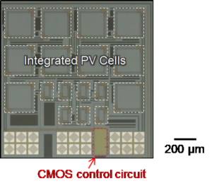
The PV-powering approach is also advantageous from the viewpoint of simple and small device design. The PV cells and the electric circuits (CMOS integrated circuits) can be integrated onto one Si chip. Fig. 3 shows a Si chip with integrated circuits and PV-cells [6]. It can receive light, generate electric power, and control the operation. The only two external components of an ultra-small implantable optogenetic stimulator are a chip capacitor that accumulates electricity, and a blue LED that generates blue stimulation light. Details of the circuit and device design are presented in refs. [6, 7].
Fig. 4 shows (a) structure, (b) outlook, and (c), (d) operational scenes of the present implantable optogenetic stimulator [6]. The typical volume and weight of the device are 1 mm3 and 2.3 mg, respectively.
We have successfully demonstrated device in-vitro functionality [6] and bench-top performance [6,7]. The device can generate light pulses with an intensity range of 1–10 mW/mm2. The duration of the pulses is in the range from sub-milliseconds to 5ms and operation frequencies are 1–10 Hz. The pulse duration and operation frequency are in trade-off, and the product of the pulse duration and the frequency is defined by the capacitance. Therefore, the averaged stimulation power is derived from the product of the available IR power and conversion efficiency, as in other operation schemes such as RF-powering and molecular-based up-conversion. The merits of our approach are greater suitability for smaller sizes than RF-powering, and significantly lower IR illumination than molecular-based up-conversion. Because the present implantable stimulator accumulates power from IR light, it can generate a blue stimulation light with a higher intensity than the powering IR light. On the other hand, molecular-based up-conversion materials always require higher IR light power than blue light.
We are currently upgrading the design of the device regarding various aspects of functionality and performance. The future work includes improvement of power-transfer efficiency, regulation of stimulation light power, and implementation of improved controllability, such as by external triggering. We are also improving the physical strength of the device for better usability in animal experiments.
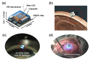
Fig. 4 (a) Structure, (b) outlook, and operation scenes of the implantable optogenetic stimulator on (c) slide glass, and (d) mouse brain. All the animal procedures were conducted in accordance with the animal care and experimentation guidelines of the Nara Institute of Science and Technology. The movie for (c) is available at:
https://aip.scitation.org/doi/10.1063/1.5024243
Acknowledgements
This work was supported in part by the Japan Science and Technology Agency under PRESTO #JPMJPR1689, and by the Japan Society for the Promotion of Science under KAKENHI #17H02222 and 19K22844. The CMOS chips were designed with the support of the VLSI Design and Education Center (VDEC), University of Tokyo, in collaboration with the Cadence Corporation and the Mentor Graphics Corporation.
References
[1] H. M. Lee, H. Park, and M. Ghovanloo, IEEE J. Solid-State Circuits 48, 2203 (2013). [2] A. J. Yeh, J. S. Ho, Y. Tanabe, E. Neofytou, R. E. Beygui, and A. S. Y. Poon, Appl. Phys. Lett. 103, 163701 (2013). [3] K. L. Montgomery, A. J. Yeh, J. S. Ho, V. Tsao, S. Mohan Iyer, L. Grosenick, E. A. Ferenczi, Y. Tanabe, K. Deisseroth, S. L. Delp, and A. S. Y. Poon, Nat. Methods, 12, 969 (2015). [4] S. Il Park, G. Shin, A. Banks, J. G. McCall, E. R. Siuda, M. J. Schmidt, H. U. Chung, K. N. Noh, J. G.-H. Mun, J. Rhodes, M. R. Bruchas, and J. a Rogers, J. Neural Eng. 12, 056002 (2015). [5] N. Wuthibenjaphonchai, M. Haruta, T. Noda, K. Sasagawa, T. Tokuda, M. Sawan, and J. Ohta: Jpn. J. Appl. Phys. 57, 04FM05 (2018). [6] T. Tokuda, T. Ishizu, W. Nattakarn, M. Haruta, T. Noda, K. Sasagawa, M. Sawan, and J. Ohta: AIP advances 8, 045018 (2018). [7] T. Tokuda, T. Ishizu, N. Wuthibenjaphonchai, M. Haruta, T. Noda, K. Sasagawa, M. Sawan, and J. Ohta, Sens. Mater. 30, 2343 (2018).
Shot biography & Photos
 Takashi Tokuda (M’08) received his B.E. and M.E. degrees in Electronic Engineering from Kyoto University, Kyoto, Japan, in 1993 and 1995, respectively. He received his Ph.D. degree in Materials Engineering from Kyoto University in 1998. He had been an assistant professor in 1999-2008, and an associate professor in 2008-2019 at the Graduate School of Materials Science, Nara Institute of Science and Technology (NAIST). Since 2019, he is a professor in Tokyo Institute of Technology. His research interests include CMOS image sensors, implantable devices, wireless technology, and IoT.
 Makito Haruta received his B.E. degree in bioscience and biotechnology from Okayama University, Okayama, Japan, in 2009, and M.S. in biological science from Nara Institute of Science and Technology (NAIST), Nara, Japan, in 2011, and Dr. Eng. in material science from NAIST in 2014. He was a postdoctoral fellow at NAIST from 2014 to 2016. He was appointed as an assistant professor in NAIST in 2016. His research interests include brain imaging devices for understanding brain functions related to animal behaviors.
 Kiyotaka Sasagawa (M’08) received his B.S. degree from Kyoto University, Kyoto, Japan, in 1999 and the M.E. and Ph.D. degrees in materials science from Nara Institute of Science and Technology (NAIST), Nara, Japan, in 2001 and 2004, respectively. From 2004 to 2008, he was a researcher with the National Institute of Information and Communications Technology, Tokyo, Japan. In 2008, he was appointed as an assistant professor in NAIST. He is an associate professor since 2019. His research interests involve bioimaging, biosensing, and electromagnetic field.
 Jun Ohta (M’97, SM’15) received his B.E., M.E., and Dr. Eng. degrees in applied physics, all from the University of Tokyo, Japan, in 1981, 1983, and 1992, respectively. In 1983, he joined Mitsubishi Electric Corporation, Hyogo, Japan. From 1992 to 1993. In 1998, he joined Nara Institute of Science and Technology (NAIST), Nara, Japan, as an associate professor. He is a professor since 2004. His research interests include smart CMOS image sensors for biomedical applications and retinal prosthetic devices.


