Xiaolin Yang and Carolina Mora Lopez
Monitoring large groups of neurons in various brain regions, including superficial and deep structures, is crucial for advancing neuroscience research on cognition, motor control, behavior, among other areas [1], [2]. Current extracellular CMOS high-density neural probes are becoming the new standard in electrophysiology, allowing for simultaneous recording with excellent spatial and temporal resolution [3]–[5]. However, there is still a demand for neural recording technologies that can access a significantly larger number of neurons, allowing for the decoding of more complex motor, sensory, and cognitive tasks. To achieve this, it is necessary to develop neural probes with much higher number of channels, which requires the design of readout circuits that meet several requirements, including: i) area- and power-efficiency, ii) low noise to capture weak neural signals, iii) capability to interface with large-impedance and high-DC-offset electrodes, and iv) tolerance to artifacts caused by movement or concurrent electrical stimulation.
To address the design requirements mentioned above, the most common neural readout architecture uses multi-channel AC-coupled amplification stages followed by a multiplexed analog-to-digital converter (ADC) [3], [4]. This approach can be further optimized to reduce the channel area, thereby increasing the channel density [5]. However, the potential for area reduction is limited due to the need for large transistors to minimize the flicker noise. In recent years, direct-digitization neural readouts have been proposed to overcome this limitation, by utilizing noise shaping and oversampling techniques [6]–[12].
In our previous work [8], we propose a DC-coupled 2nd-order ∆2-∑ ADC to achieve significant area reduction. Here, chopping modulation is implemented to improve the noise performance. A new bootstrapping scheme is introduced to nullify the impact from the parasitic capacitor of the input pair transistors, thereby achieving high input impedance (663 MΩ @ 10 Hz). Furthermore, a large dynamic range (>140 mVpp) is achieved to accommodate electrode DC offsets (EDOs) and stimulation artifacts. A 16-channel prototype ASIC was successfully demonstrated in in vitro experiments using iCell Cardiomyocytes cells cultured on a multi-electrode array (see Fig. 1).
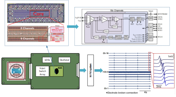
Fig.1. Die photo of the prototype ASIC (top left) and system architecture (top right) of the ASIC reported in [8]; in vitro experimental setup and results (bottom).
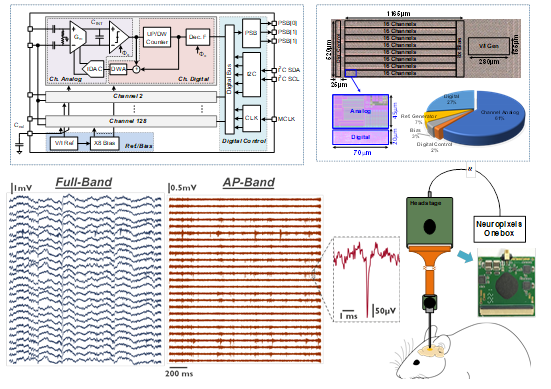
Fig.2. Overall architecture of the 128-channel ASIC reported in [11] (top left) and die photo with area partitioning (top right); in vivo experimental results and setup including a headstage and a passive neural probe (bottom).
References:
[1] N. A. Steinmetz et al., “Neuropixels 2.0: A miniaturized high-density probe for stable, long-term brain recordings,” Science, vol. 372, no. 6539, p. eabf4588, 2021 [2] J. J. Jun et al., “Fully integrated silicon probes for high-density recording of neural activity,” Nature, vol. 551, no. 7679, pp. 232–236, 2017. [3] C. Mora Lopez et al., “A Neural Probe With Up to 966 Electrodes and Up to 384 Configurable Channels in 0.13 μm SOI CMOS,” IEEE Trans Biomed Circuits Syst, vol. 11, no. 3, pp. 510–522, Jun. 2017. [4] S. Wang et al., “A Compact Quad-Shank CMOS Neural Probe With 5,120 Addressable Recording Sites and 384 Fully Differential Parallel Channels,” IEEE Trans Biomed Circuits Syst, vol. 13, no. 6, pp. 1625–1634, 2019. [5] D. Y. Yoon, S. Pinto, S. W. Chung, P. Merolla, T. W. Koh, and D. Seo, “A 1024-Channel Simultaneous Recording Neural SoC with Stimulation and Real-Time Spike Detection,” in IEEE Symposium on VLSI Circuits, Digest of Technical Papers, 2021. [6] D. Wendler et al., “A 0.0046-mm2 Two-Step Incremental Delta-Sigma Analog-to-Digital Converter Neuronal Recording Front End With 120-mVpp Offset Compensation,” IEEE J Solid-State Circuits, pp. 1–12, 2022. [7] D. De Dorigo et al., “Fully Immersible Subcortical Neural Probes With Modular Architecture and a Delta-Sigma ADC Integrated Under Each Electrode for Parallel Readout of 144 Recording Sites,” IEEE J Solid-State Circuits, vol. 53, no. 11, pp. 3111–3125, Nov. 2018. [8] S. Wang et al., “A Compact Chopper Stabilized Δ-ΔΣ Neural Readout IC With Input Impedance Boosting,” IEEE Open Journal of the Solid-State Circuits Society, vol. 1, pp. 67–78, 2021. [9] C. Kim, S. Joshi, H. Courellis, J. Wang, C. Miller, and G. Cauwenberghs, “Sub-μ Vrms-noise Sub-μ W/Channel ADC-direct neural recording with 200-mV/ms transient recovery through predictive digital autoranging,” IEEE J Solid-State Circuits, vol. 53, no. 11, pp. 3101–3110, 2018. [10] H. Kassiri et al., “Rail-to-Rail-Input Dual-Radio 64-Channel Closed-Loop Neurostimulator,” IEEE J Solid-State Circuits, vol. 52, no. 11, pp. 1–18, 2017. [11] X. Yang et al., “An AC-Coupled 1st-Order Δ-ΔΣ Readout IC for Area-Efficient Neural Signal Acquisition,” IEEE J Solid-State Circuits, vol. 58, no. 4, pp. 949–960, 2023. [12] X. Huang et al., “Actively Multiplexed μECoG Brain Implant System With Incremental-ΔΣ ADCs Employing Bulk-DACs,” IEEE J Solid-State Circuits, vol. 57, no. 11, pp. 3312–3323, 2022.