Communicated by Dr. Jun Wang
December 2021
Linran Zhao1, Wen Li2, Maysam Ghovanloo3, Yaoyao Jia1*
1Department of Electrical and Computer Engineering, The University of Texas at Austin
2Department of Electrical and Computer Engineering, Michigan State University
3Silicon Creations Inc.
*Corresponding author: yjia@austin.utexas.edu
There is an increasing realization that the majority of brain functions relate to a large distributed network of neurons that are spread over different interconnected regions of the brain [1]. Thus, neural recording and modulation of the future will require the ability to simultaneously interface with multiple neural sites distributed over a large brain area. Traditional methods for modulating neuronal function have relied on direct stimulation by tiny electrodes, which effectiveness is undermined by the limited spatial and temporal precision with which individual cells can be selectively targeted [2]. The emergence of optogenetic stimulation provides distinct advantages over electrical stimulation, such as cell-type specificity, sub-millisecond temporal precision, and rapid reversibility. Optogenetic neuromodulation has the potential to revolutionize the study of how neurons operate as members of larger networks and may ultimately help patients suffering from neurological disorders [3]. Hence, we aspire to design a distributed wireless neural interface framework to stimulate large-scale neuronal ensembles over large brain areas. The distributed framework includes an array of tiny, wireless, and highly efficient implants, each of which operates autonomously to stimulate neural activities.
The LED is a commonly used light source for optogenetic neuromodulation because of low cost, power efficiency, stable illumination, compact size, fast response, and compatibility with circuitry [3]. Recently, a few miniature implants have been presented for neuromodulation with an impressive reduction in the device size [4-9]. Despite these advancements, designing miniature implants still face several challenges. Device miniaturization is required to minimize invasiveness to the surrounding tissue and thereby enable chronic implantation. As device size shrinks, it would impose a limit on the amount of received power and the size of the antenna, which in turn makes it challenging to maintain the continuity and integrity of wireless power and data transmission. The highly constrained power budget prevents these devices from performing power-consuming applications, such as optogenetic stimulation. Effective optogenetic neuromodulation requires high instantaneous current delivered to the LED, in the order of several mA to tens of mA, for the intensity of the resulting flash of light to surpass the optogenetic neuromodulation threshold [10]. Thus, operating optogenetic stimulation is a major challenge for an implant with limited power budget. On the other hand, a large amount of wireless power needs to be delivered to energize a power-consuming device. This will result in excessive heat dissipation, considerable radiation, and large electromagnetic interference with surrounding instruments. In sum, there is always a conflicting tradeoff among size, power budget, and device functions.
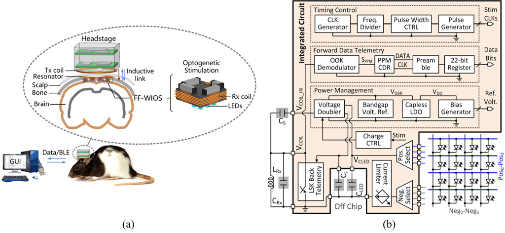
Figure 1. (a) Conceptual view of the system setup for operating multiple FF-WIOS devices, distributed on a freely moving rat brain. (b) A simplified system architecture of the FF-WIOS SoC.
We have demonstrated a mm-sized, free-floating, wirelessly powered, implantable, 16-channel optogenetic stimulation (FF-WIOS) device [11]. Figure 1(a) shows the conceptual view of multiple FF-WIOS devices distributed on the surface of a freely behaving rat brain. The FF-WIOS includes a system-on-chip (SoC), surface-mount device (SMD) capacitors (0201), a receiver (Rx) coil, and a 4×4 LED array, all mechanically supported on a polyimide substrate. The wire-wound Rx coil, LRx, together with a transmitter (Tx) coil and a high-Q resonator form a 3-coil inductive link. The Rx coil encompasses the SoC. The resonator encompasses one or more FF-WIOS implants roughly in the same plane. The Tx coil is part of the external headstage. The headstage includes a class-E power amplifier, which is controlled by a microcontroller (MCU) (CC2541, Texas Instruments) to deliver power from battery to the FF-WIOS through the 3-coil link at 60 MHz. To wirelessly control the FF-WIOS, stimulation parameters, which are set in a graphical user interface (GUI) running on a nearby PC, are sent to the headstage MCU via Bluetooth Low Energy (BLE) link and then relayed to the FF-WIOS through the 3-coil link by on-off-keying (OOK) the power carrier signal. The rectified voltage on the FF-WIOS is also digitized, as a measure of the received power on the SoC. The digitized data is sent back to the headstage via load-shift-keying (LSK) to close the power control loop and eventually send to the PC via BLE for real-time display.
The FF-WIOS SoC block diagram is shown in Figure 1(b). A key challenge in the FF-WIOS SoC design is to efficiently utilize the limited power budget to deliver high pulsed current to LED for effective optogenetic neuromodulation. Thus, we design a switched-capacitor-based stimulation (SCS) architecture in the FF-WIOS SoC. More specifically, a voltage doubler periodically charges a storage capacitor, CLED, from the inductive link. A charge control unit sets the target charging voltage at 5 V. At the onset of stimulation, CLED is detached from the charger and dumps its charge to a designated LED without loading the inductive link. A current limiter is added to limit the maximum current flowing through the target LED.
Figure 2(a) depicts the steps for microassembly of the FF-WIOS. Copper traces are patterned on both sides of the polyimide substrate to form interconnections between the wire bonded SoC die, LED pads, and SMD caps. The LEDs (220×270×50 µm3, TR2227TM, Cree) are mounted on their pads using low melting point solder and then encapsulated using Parylene-C. The FF-WIOS SoC is fixated in the center of the substrate for wire bonding, followed by coating using medical grade epoxy. The SMD 0201 capacitors are mounted on the periphery of the SoC die using silver conductive epoxy. The Rx coil is then wire wound around the SoC die with its terminals connected to one of the SMD capacitors by silver conductive epoxy to form the LC-tank resonating at the power carrier frequency. Finally, the FF-WIOS device is sealed with Parylene-C and PDMS. In Figure 2(b), the FF-WIOS device has dimensions and weight of 2.5×2.5×1.5 mm3 and 15 mg, respectively.
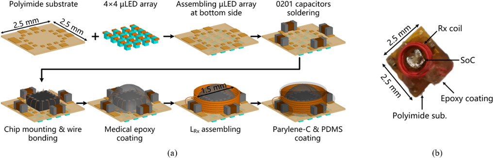
Figure 2. (a) The fabrication and microassembly process of the FF-WIOS device. (b) The implementation of the FF-WIOS device.
The development of the current FF-WIOS prototype is an important step towards realization of the distributed neural interface concept. While the size and weight of the current headstage and FF-WIOS are tailored for the rat model, the same concept can be used to design the headstage and FF-WIOS for other animal models. Our next step is to further reduce the size of the FF-WIOS device, from a 2.5-mm3 to 1-mm3. Instead of assembling all the components on the polyimide substrate, we will fold the substrate. To do so, we plan to use flexible Parylene-C material. The Parylene-C substrate that carriers the 4×4 LED array will be attached to the bottom of the SoC die and then folded along the side walls of the SoC die to connect with the pads on the top of the SoC die.
References
- Jia, Y. et al. A mm-Sized Free-Floating Wireless Implantable Opto-Electro Stimulation Device. Micromachines. 2020;11(6):621.
- Santaniello, S. et al. Closed-loop control of deep brain stimulation: a simulation study. IEEE Transactions on Neural Systems and Rehabilitation Engineering. 2010;19(1):15-24.
- Jia, Y. et al. Wireless opto-electro neural interface for experiments with small freely behaving animals. Journal of Neural Engineering. 2018;15(4):046032.
- Tokuda, T. et al. 1 mm3-sized optical neural stimulator based on CMOS integrated photovoltaic power receiver. AIP Advances. 2018;8(4):045018.
- Shin, G. et al. Flexible near-field wireless optoelectronics as subdermal implants for broad applications in optogenetics. Neuron. 2017;93(3):509-21.
- Montgomery, K. L. et al. Wirelessly powered, fully internal optogenetics for brain, spinal and peripheral circuits in mice. Nature Methods. 2015;12(10):969-74.
- Noh, K. N. et al. Miniaturized, battery‐free optofluidic systems with potential for wireless pharmacology and optogenetics. Small. 2018;14(4):1702479.
- Charthad, J. et al. A mm-sized wireless implantable device for electrical stimulation of peripheral nerves. IEEE Transactions on Biomedical Circuits and Systems. 2018;12(2):257-70.
- Lee, J. et al. Neural recording and stimulation using wireless networks of microimplants. Nature Electronics. 2021;4:604-614.
- Stark, E. et al. Diode probes for spatiotemporal optical control of multiple neurons in freely moving animals. Journal of Neurophysiology. 2012;108(1):349-63.
- Jia, Y. et al. A mm-sized free-floating wirelessly powered implantable optical stimulation device. IEEE Transactions on Biomedical Circuits and Systems. 2019;13(4):608-18.
Author Biographies
 Linran Zhao received his B.S. degree from the University of Electronic Science and Technology of China, Chengdu, China, in 2017 and his M.S. degree from the University of California, Irvine, in 2019. During 2019-2020, he worked as an analog design engineer in ASML, San Jose, CA. He is currently pursuing his Ph.D. degree at The University of Texas at Austin. His research interest includes analog/mixed-signal IC for bio-implantable devices and applications.
 Wen Li (S’03-M’09-SM’14) received her Ph.D. (2009) and M.S. (2004) in Electrical Engineering from California Institute of Technology. Dr. Li is currently a professor of Electrical and Computer Engineering at Michigan State University. Her research focuses on MEMS/NEMS, neuroprosthetic devices, micro/nano sensors and actuators, nanoelectronics, and microsystem integration and packaging technologies.
 Maysam Ghovanloo received the B.S. degree in electrical engineering from the University of Tehran, the M.S. degree in biomedical engineering from the Amirkabir University of Technology, and the M.S. and Ph.D. degrees in electrical engineering from the University of Michigan in Ann Arbor in 2003 and 2004, respectively. From 2004 to 2007, he was an Assistant Professor with the Department of Electrical and Computer Engineering, North Carolina State University, Raleigh, NC. From 2007 to 2019, he was a Professor with the School of Electrical and Computer Engineering at Georgia Tech. Currently he is generating intellectual property (IP) in advanced integrated circuits at Silicon Creations, Atlanta, GA. He has coauthored over 250 peer-reviewed publications on implantable microelectronic devices, circuits and microsystems, and modern assistive technologies, and holds 11 U.S. patents. He is a Fellow of the IEEE and a recipient of the National Science Foundation CAREER Award, Tommy Nobis Barrier Breaker Award for Innovation, and the Distinguished Young Scholar Award from the Association of Professors and Scholars of Iranian Heritage. He was the General Chair of the 2015 IEEE Biomedical Circuits and Systems (BioCAS) Conference in Atlanta, GA. He is an Associate Editor of the IEEE Transactions on Biomedical Circuits and Systems and served as an Associate Editor for the IEEE Transactions on Circuits and Systems-II and IEEE Transactions on Biomedical Engineering.
 Yaoyao Jia (S’14-M’19) received her Ph.D. in Electrical Engineering from the Georgia Institute of Technology in August 2019. Dr. Jia was an assistant professor in the Department of Electrical and Computer Engineering at North Carolina State University from August 2019 to August 2021. She is currently an assistant professor in the Department of Electrical and Computer Engineering at the University of Texas at Austin. Her research focuses on analog/mixed-signal integrated circuits, wireless power and data transmission, energy harvesting, implantable and wearable biomedical devices, and neural interface implants. Currently she is appointed as a Fellow of Silicon Laboratories Chair. She is serving as the Associate Editor of IEEE Transactions on Biomedical Circuits and Systems (TBioCAS). She is also serving on the Technical Program Committee of IEEE Biomedical Circuits and Systems Conference (BioCAS) and IEEE Custom Integrated Circuits Conference (CICC).