Communicated by Dr. Yiwen Wang
December 2021
Leilei Gu1, Yucheng Ding2, Zhiyong Fan2 Senior Member IEEE
1 Qingyuan Research Institute, School of Electronic Information and Electrical Engineering, Shanghai Jiao Tong University
2 Department of Electronic & Computer Engineering, The Hong Kong University of Science and Technology
Email: leilei.gu@sjtu.edu.cn, eezfan@ust.hk
“To see is to believe”. High-performance imaging devices are essential in society, particularly in the current age of Artificial Intelligence (AI) +. The biological eyes have been polished by natural selection for millions of years and their function has been verified by the diverse environment. Learning from the masterpiece of nature is therefore a shortcut to improve our manmade systems. As one of the wisest creatures in nature, human eyes are advanced image sensing systems with superiorities such as high resolution, wide field-of-view (FoV), high energy efficiency, and strong accommodations. Their high performance originates from the combined effect of a vastly flexible optical system, high-density and sensitive photoreceptor arrays, and powerful neural networks from both retina and cortex. The human eyes have a spherical shape with a hemispherical retina. A hemispherical shape matches well with the Petzval surface, which is the theoretical focal plane of the spherical lens, leading to clear and sharp imaging. In regular cameras, to mitigate the mismatching in planar structure, a delicate lens array has to be inserted to gradually bend the focal plane into quasi-flat. In our cell phones, there are 10-16 lens (1). With a well-designed hemispherical image sensor, high-quality imaging with a simple structure can be achieved.
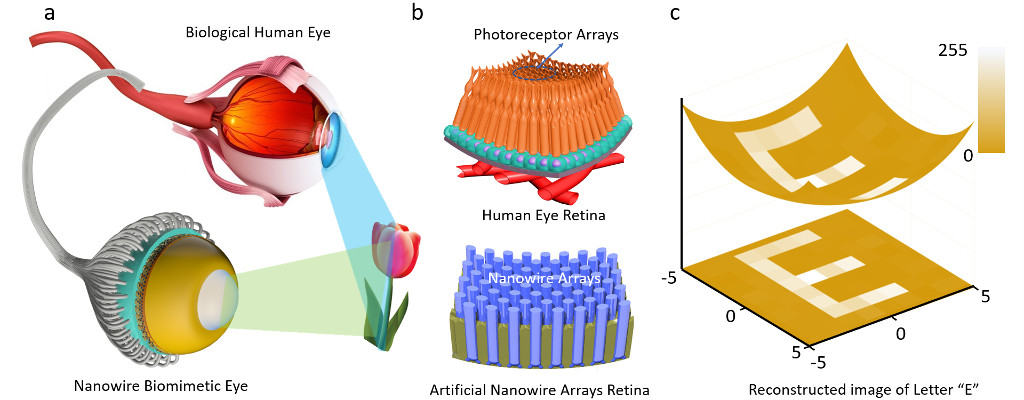
Figure 1. Structure of NW array biomemetic eye. (a) the overall structure of biomimeitic and human eyes. (b) Structure of biological and NW array artificial retina. (3) Representative imaging result of biomimetic eye with input pattern of Letter “E”.
In spite above advantages, the mainstream of today’s image sensors, charge-coupled device (CCD) and complementary metal-oxide semiconductor (CMOS), still have a planar architecture. This originates from the planar semiconductor fabrication process and the rigid materials(2,3). Recently, we have invented a brand-new strategy to build a spherical biomimetic eye, which has a structure very close to that of human eyes (Fig.1a). The hemispherical nanowire (NW) array is the core component of this device, which converts the incident light into electrical signals, mimicking the function of retina in biological eyes (Fig.1b). Compared to conventional image sensors, the templated assisted grown NWs have unique properties in favor of imaging performance: 1) The NW arrays have balanced optoelectronic properties and thus can increase the overall photodetection performance. 2) The NWs are highly integrated and each of them are isolated by the insulative Alumina. Therefore, one single NW can work independently as an individual pixel and the whole device can achieve ultrahigh resolution imaging beyond human eyes. 3) The hemispherical shape of NW arrasy matches well with the optical system, enabling high quality imaging with simplified structure. The NW array-based optoelectronics has combined the fundamental scientific problems of light-material interaction, delicate engineering issues in integration and the beauty of art from nature. We are attracted by this field for over 10 years, and accomplished fruitful results reported by top scientific journals such as Nature,(4) Nature Communications,(5) Advanced Materials(6) and Nano Letters(7) etc. We do believe that more innovative results will come out along this direction.
To realize ultrahigh resolution imaging, the individual NW has to be further assembled into complete photodetectors, which function as individul pixels of an image sensor. By collecting the current of the pixels, the incident light pattern can be reconstructed into a gray-scale image (Fig.1c). In our device, all the pixels are designed to share one common front electrode, and looking for proper back contact integration strategy, particularly on the hemispherical substrate, has become the most challenging part of the whole project. We have tried many different ways such as direct wire bonding, copper wire bundle bonding, and the commercial Utah electrodes array. After millions of times of error trials, we have finally developed two technologies, which have the potential for large-scale and high-density integration. One is the liquid metal fiber strategy demonstrated above (Fig.1a). It is facial but may be challenging to scale down to a micrometer scale. The other is “magnetic field assisted microneedle alignment strategy”. In this method, a sharpened needle was inserted into the exposed metal NW forest to contact with NWs. Each microneedle contacts with only 3 NWs, resulting in a small device footprint of 1 µm2. Due to the divergence of the magnetic field, the needles form strong contact with the hemispherical substrate and this process is particullay fit for spherical and other nonplanar substrates.
In our work, we have developed new material system and fabrication process to achieve biomimetic electrochemical eyes. Although they have demonstrated appealing potential in many aspects, more efforts in optimization are desired to make them come true. In addition, to push them one step further toward practical applications, the high-performance sensors have to be well combined with brains, artificial or biological brain, to form a complete biomimetic visual system. Figure 2 demonstrates two represeantive fileds that can be greatly improved by the biometic eyes, the machine vision and visual prostheses. Particulary in visual prostheses, the current bionic eyes suffer from series of challenges such as low visual acuity, small FoV and poor long sterm stability etc (8-10). Many of these issues can be well addressed by fabricating high-density, large-area and hemispherical arrays artifical retina.
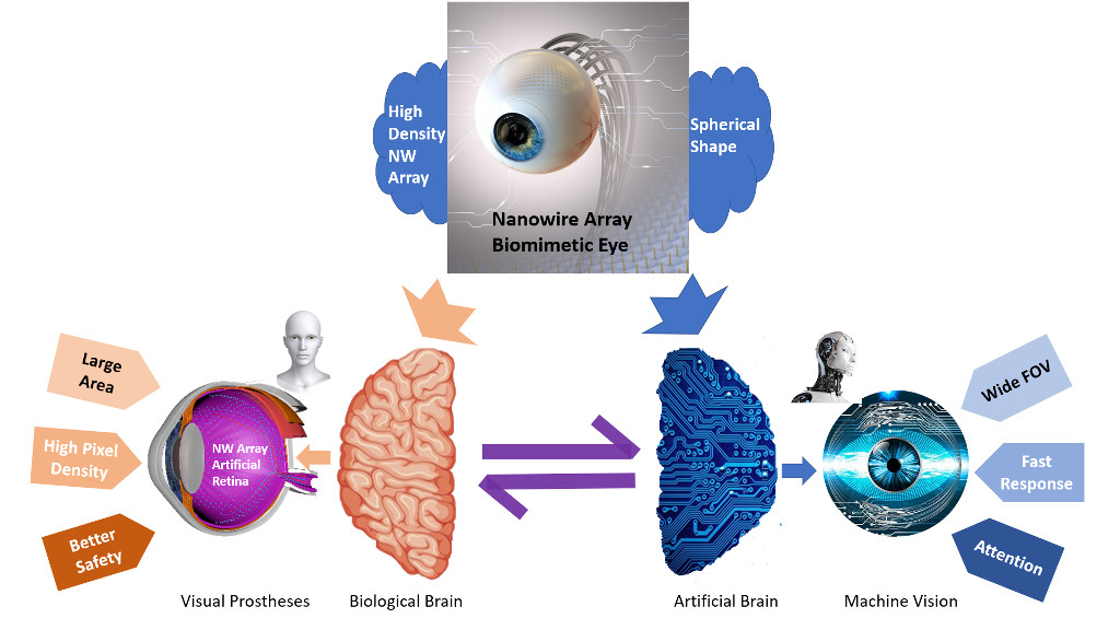
Figure 2 The repretentative potential of spherical NW array biomimetic eyes in machine vision and visual prosthese.
In all, in our device, the high density NWs have enabled high resolution imaging beyond human eyes. From planar to spherical, it is a revolutionary leap for an imaging device opening vast opportunities from bringing light back for the visually impaired to viewing the world in panorama. Owing to the profound social and technological impact of our work, it has attracted tremendous public attention with top 10% ranking among all papers published in Nature of the same age. The positive feedback from the public has given us more confidence and motivation to make more efforts towards these dreams.
References
- Guenter et al. “Highly curved image sensors: a practical approach for improved optical performance”, Opt. Express 25, 13010 (2017).
- Ko et al. “A hemispherical electronic eye camera based on compressible silicon optoelectronics”, Nature 454, 748 (2008).
- Kim et al. “An aquatic-vision-inspired camera based on a monocentric lens and a silicon nanorod photodiode array”, Nat. Electron. 3, 546 (2020).
- Gu et al. “A biomimetic eye with a hemispherical perovskite nanowire array retina,” Nature 581, 278 (2020).
- Zhang et al. “Efficient metal halide perovskite light-emitting diodes with significantly improved light extraction on nanophotonic substrates”, Nat. Commun., 10, 727 (2019).
- Gu et al. “3D Arrays of 1024‐Pixel Image Sensors based on Lead Halide Perovskite Nanowires”, Adv. Mater. 28, 9713 (2016).
- Waleed et al. “All Inorganic Cesium Lead Iodide Perovskite Nanowires with Stabilized Cubic Phase at Room Temperature and Nanowire Array-based Photodetectors”, Nano Lett. 17, 4951-4957 (2017).
- Lee, et al. “Ultra-high responsivity, silicon nanowire photodetectors for retinal prosthesis”, in IEEE 25th International Conference on Micro Electro Mechanical Systems (MEMS) 1364-1367 (2012).
- D. Weiland and M. S. Humayun, “Visual Prosthesis”, in Proceedings of the IEEE, 96, 1076-1084 (2008).
- Bosse et al. “In vivo photovoltaic performance of a silicon nanowire photodiode–based retinal prosthesis”, Investig. Ophthalmol. Vis. Sci. 59, 5885-5892 (2018).
Author Biographies
 Prof. Leilei Gu received his Bachelor and Master degrees from Fudan University in 2008 and 2011, respectively. He earned his Ph.D in 2016 from the Hong Kong University of Science and Techonology (HKUST). From 2016 to 2020, he worked in HKUST as a postdoc fellow. In November 2020, he joined Shanghai Jiao Tong University as a tenure-track Associate Professor. His research focuses on interdisciplinary research of biomimetic nanostructures and intelligent sensing. Prof. Gu has published over 30 journals on top scientific journals such as Nature, Nature Communications and Advanced Materials. His representative work has been highlighted as “Nature Research Highlights” and “Nature Hot Topics”, and featured as “2020 Top 10 Research Progress on Semiconductors in China” and “2020 Top 10 Innovation News in Hong Kong”.
 Mr. Yucheng Ding received BSc. in chemistry from Nanjing University in 2020, and entered the Hong Kong University of Science and Technology in the same year to pursue the PhD. degree in electronic and computer engineering. His research interests focus on the application of perovskite optoelectronic devices, the development and integration of biomimetic devices, etc. He has published papers in Journal of Power Sources and other journals as a co-author.
 Prof. Zhiyong Fan received his B.S. and M.S. degree from Fudan University, China. He received Ph.D. degree from University of California, Irvine in 2006. From 2007 to 2010, he worked in University of California, Berkeley as a postdoctoral fellow in department of Electrical Engineering and Computer Sciences, with a joint appointment with Lawrence Berkeley National Laboratory. In May 2010, he joined the faculty of Hong Kong University of Science and Technology and currently he is a professor at Department of Electronic and Computer Engineering. Prof. Fan’s research interests are on design and fabrication of novel nanostructures and nanomaterials for high performance optoelectronics, energy harvesting devices and sensors. He has won a number of awards including IEEE Sensor Research Scholarship Award, UC Berkeley BSAC Outstanding Research Presentation Award, HKUST SENG Young Investigator Award, Research Excellence Award, HKUST President’s Award and Innovation Award, 2018 ESI Highly Cited Researcher etc. He currently serves as an editorial board member of NPG Scientific Reports and Springer Nanoscale Research Letters, and Journal of Semiconductors.